

CENTERA Leader Prof. W. Knap Main Scientific Activities 1980 – 2020
Prof. W. Knap Main Scientific Activities 1980 – 2020 – short version.
My research activity was concentrated on Solid State Physics. I studied, transport and optical (from visible till far Infrared/THz) properties of semiconductors using high pressure and/or high magnetic fields in extreme conditions. An important part of my scientific experience comes from the fact that I was working in many different laboratories and research centers.
1979-1987 : Institute of Physics – Solid State Group University of Warsaw.
1985-1986 : Innsbruck and Leoben groups of Semiconductor Physics Austria.
1989-1990 : Grenoble High Magnetic Field Laboratory CNRS-SNCI Grenoble.
1991-1992 : Pulsed Magnetic Field Laboratory Toulouse (France).
1999-2001 : Terahertz Center of Rensselaer Polytechnic Inst. Troy-New York (USA).
2007-2019 : Research. Inst. of Elec. Com. –RIEC Tohoku University – Sendai (Japan).
1988-2020: Centre National Researche Scientifique - Montpellier (France).
2000-2020 : Institute of High Pressure Physics – Polish Academy of Sciences.
This important mobility was one of the factors stimulating the frequent changing of the research subjects and experimental techniques. The simplified list of important research subjects with short comments is given below:
1) Thermomagnetic and galvanomagnetic phenomena in narrow/zero gap semiconductors.
Investigation of the interaction of the narrow gap semiconductors (HgTe and InSb) with Far Infrared Radiation was the main subject of my master and PhD dissertations. My Ph.D. thesis completed at the University of Warsaw under the supervision of Prof. M. Grynberg in 1985 had the title “Thermomagnetic and galvanomagnetic effects induced by Far Infrared Radiation in HgTe and InSb in high magnetic fields”.
2) Resonant impurity states in zero gap semiconductors.
This work was done in collaboration with Prof. G. Bauer, Leoben (Austria). The subject was related to Fourier spectroscopy far infrared transmission studies of extremely thin HgTe samples with different doping. We have shown the existence of the optical singularities related to the impurity states resonant with the conduction band of n-type HgTe.
3) Nonlinear transport and routes to chaotic oscillations in semi-insulating GaAs.
This research was on the border between physics and advanced mathematics. It was based on experiments showing a clear “period doubling route to chaos” (Warsaw and Montpellier).
4) Hot electrons in high magnetic fields – Landau level emission.
This project was realised under the supervision of Prof. E. Gornik (Innsbruck – Austria and Munich - Germany).
I continued this research in Warsaw and Montpellier constructing 2 cyclotron resonance spectrometers.
5) Paramagnetic resonance in high magnetic fields: spin relaxation mechanism.
My work in this field was a participation in the construction of the high field EPR spectrometer in Grenoble High Magnetic Field Laboratory (Grenoble). Important results on spin relaxation in the Si:P and heavily doped Silicon were obtained. Spin relaxation rates as a function of temperature and magnetic field were determined and a new relaxation mechanism specific to high magnetic fields was identified.
6) Blocked Impurity Band Detectors of Infrared Radiation (BIBs).
These studies were related to the construction of a new type of Far Infrared detectors that are insensitive to ionizing radiation. I have also installed a Fourier Spectrometer based optical test system. Laboratory of Pulsed Magnetic Fields, Toulouse.
7) Cyclotron Emission from two-dimensional electron systems.
This was the continuation -for 2DEG systems of the project started in Innsbruck and Warsaw (Montpellier). It was the development of the system and the introduction of the high pressure cell. I have obtained the first results on the 2DEG effective mass change with hydrostatic pressure.
8) Quantum Transport - Weak localisation and antilocalization.
Important research project – stimulated by theoretical support of Russian scientists from St. Petersburg and Moscow – allowed the discovery of the universal weak localization and identification of major spin splitting/relaxation mechanisms responsible for weak anti-localisation phenomenon. Part of the work leads to a common Ph.D. thesis between Montpellier and Warsaw Universities.
9) Semiconductor based gas detectors.
This work was made in collaboration with Schlumberger Industries. The first important project with direct applications for industry, Ph.D. thesis of H. Alause and an international Patent, were linked to this field of research.
10) Cyclotron Resonance and Infrared reflectivity studies of GaN and SiC wide gap semiconductors and their heterojunctions.
We have determined by cyclotron resonance infrared reflectivity and transport methods effective masses and other band parameters of wide band semiconductors GaN and SiC. We studied then the details of the conduction band of 2DEG in GaN/AlGaN heterostructures. This work was done in collaboration with Unipress (Warsaw), HMFL in Grenoble, le Service des Champs Pulsés de Toulouse, High Magnetic Field Laboratory – Tallahassee (USA), RPI –Troy-New York (USA), and APA Optics (USA).
11) Diamond Anvils investigation of High pressure-induced metal semiconductor transition in bulk GaN.
The aim of this research was the understanding of the mechanism of doping in GaN bulk that synthesized under high pressure was always n-type. Organization of fruitful collaboration Montpellier (Micro Luminescence and Raman system) Unipress – Warsaw (GaN bulk crystals) and Laboratoire de Physique des Milieux Condensés Paris VI (Diamond anvils – high pressure system).
12) Plasma wave Terahertz oscillations in nanometre size semiconductors.
This project was realized in his first phase during my stay in the USA – RPI – Troy –NY then in Montpellier, Sendai (Japan), and again in Montpellier. It is continued until now as the major research project (a more detailed description is given below).
As can be seen from the list above I have worked on many subjects related to the optical and transport properties of solids. The fact that I used different tools or approached the subject by different methods specific for different laboratories, allowed me to get important results recognized by the scientific community via invited and tutorial papers and multiple citations (H>40).
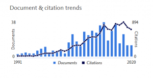
Scopus – Author’s details -Knap, W. (November 24th, 2020).
Documents: 488 Citations: 10 636 total citations by 5421 documents.
Scopus – Author’s details -Knap, W. (Nov 26, 2020).
Documents: 488 Citations: 10 636 total citations by 5421 documents.
h-index: 52 ( WEB of SCIENCE 48, Google Scholar 57).
To present more in details my scientific activity I have divided my works into two domains: A) Basic Solid State Physics and B) Applied Physics. In each of these domains, I have chosen three subjects that I consider as most important - because I had a leading/key role in their initialization and realisation and because they brought progress in the understanding of some basic phenomena in solid-state physics and/or were important for applications.
A) Basic Physics
Looking from the basic physics point of view one can choose at least three main subjects of studies:
A1. Quantum phenomena in transport: weak localisation, anti-localisation and ballistic behaviour in low dimensional systems.
A2. Wide gap nitrides and their heterojunctions: metal non-metal transition and two-dimensional gas in GaN/AlGaN heterojunctions
A3. Terahertz plasma excitations in low dimensional systems: Terahertz radiation rectification and generation by plasma confined in nanometre field-effect transistors.
The main results (“the firsts”) concerning these themes/axes are briefly presented below:
Ad-A1. Quantum phenomena in transport: weak localisation, anti-localisation and ballistic behaviour in low dimensional systems.
The main results concerning this activity are:
i) The first observation of the universal behaviour of the weak localisation. The universality of the weak localization means that for all two-dimensional systems – independently of carrier mass, scattering rates, doping levels. etc…. the quantum interference conductivity corrections should behave in the same way. More precisely they have the same functional dependence versus renormalized magnetic field.
ii) The first complete analysis of the antilocalisation behaviour. It was shown that the observed antilocalisation appearing due to the quantum interference, is controlled in an unexpectedly important way by the spin splitting of electron spectra. A theory was developed taking into account both linear and cubic wave-vector terms in spin splitting. Also, it was shown that additional linear terms appear when the quantum well itself is asymmetric (Rashba term). The results obtained allowed the determination of dominating spin-relaxation mechanisms and to improve the accuracy of determination of spin-splitting parameters in A3B5 crystals and their two-dimensional structures.
Ad-A2) Wide gap nitrides and their heterojunctions: metal non-metal transition and two-dimensional gas in GaN/AlGaN heterojunctions.
This research was performed to answer the basic nitrides related questions such as: the value of the electron effective mass and g-factor, limits of the doping, possibility of hydrostatic pressure-induced metal-non metal transition, and force of electron-phonons interactions. By the experiments:
i) Far Infrared and Infrared Reflectivity under pressure as well as by the
ii) diamond anvils high pressure Raman
iii) diamond anvils luminescence experiments we were able to answer most of these questions. Effective mass was determined and shown that it changes with carrier densities due to nonparabolicity. The polaron effect related to optical phonon free carrier’s interaction was evidenced as well as the pressure-induced metal –non-metal transition in highly doped n-GaN bulk crystals.
The GaN bulk studies were followed by a more challenging subject related to properties of two-dimensional electron gas in GaN/AlGaN heterojunctions. In collaboration with groups from the USA, Poland, and France I performed the high field experiments that lead to the:
i) The first demonstration of the existence of 2DEG gas in GaN/AlGaN heterojunctions. First observation of the Shubnikov-de-Hass as well as Quantum Hall Effects in GaN/AlGaN heterojunctions. These experiments made in tilted magnetic fields clearly demonstrated the existence of 2DEG gas.
ii) The first Far Infrared Cyclotron Resonance absorption and emission that are referenced as the first published data.
iii) The first determination of the 2DEG effective mass. This mass was different from the bulk value because of the strong polaron and non-parabolicity effects. It has been shown that effective mass can increase almost by 10% with the carrier density varying between 1012/cm2 and 1013/cm2.
By tilting magnetic fields, we were able to register the change of the pattern (phase and amplitude) of the Shubnikov-de-Haas oscillations - related to spin and cyclotron splitting and observe their anticrossing behaviour. This led to
iv) First determination of the effective g factor for 2DEG GaN/Al The value g*~2.1 was found very close to the bulk value. Contrary to observations for GaAs/AlGaAs systems, the absence of any anomalous enhancements of the spin splitting was confirmed.
v) First Quantum Hall Effect activation measurements were performed showing unusual behaviour of the quantum transport gaps and an effect of many body interactions on gap renormalization. Complete theoretical analysis of the data was performed in collaboration with V. Falco – Landau Institute – Tchernogolovka Russia. It was shown that because of the higher g* factor and higher effective mass, the spin splitting and cyclotron resonance splitting becomes comparable. This makes GaN/AlGaN system very interesting from the point of view of many body interactions.
Ad-A3) Terahertz plasma excitations in low dimensional systems: terahertz radiation rectification and generation by plasma confined in nanometer field-effect transistors.
This part of my research activity started in 1997 as a result of the collaboration with world-class theoreticians Prof. M. Dyakonov and Prof. M. Shur who predicted that constant current flow in the transistor channel with special boundary conditions can lead to a new type of instability leading to the generation of high amplitude plasma waves and Terahertz emission. They have shown also that nonlinearities related to two-dimensional plasma can lead to rectification and detection of THz radiation. Interested by these new mechanisms of THz detection and emission I started the experimental research using high sensitivity cyclotron resonance detection system for emission (built in Montpellier) and Gunn diodes based experimental system for detection (constructed during my sabbatical at RPI, Troy, New York, USA).
Main results of these studies are:
i) The first observation of the resonant THz detection by 2D plasmons in nanometre GaAs FET
ii) The first observation of the plasma instability related emission from InGaAs /InP
iii) The first room temperature broadband THz detection by nanometre Si – MOSFETs.
iv) The first room temperature THz emission from GaN/AlGaN transistor.
The most interesting basic physics problems treated in this subject concern:
i) Influence of the current on the plasma wave related detection – enhancement of the effect and narrowing of the resonances.
ii) Influence of the geometry of the channel – determination of the role of gated and ungated parts of the channel (interaction of gated and ungated 2-dimensional plasmons.
iii) Damping of Shubnikov-de-Hass oscillations at the Cyclotron and plasma resonances energy crossing in high magnetic fields.
In 2018 started CENTERA project - the main related to the THz science and technology, result obtained in the frame of this project is the first demonstration of THz amplification by plasmons in grating gate nano-structures.
We demonstrated gate voltage tuneable resonant plasmon absorption, that with an increase of the current, turns to THz radiation amplification with a gain approaching 10%. The results were interpreted using a dissipative plasmonics crystal model, which captures the main trends and basic physics of the amplification phenomena. Specifically, the model predicts that increasing current drives the system into an amplification regime, wherein the plasma waves may transfer energy to the incoming electromagnetic waves.
All results were obtained at room temperature. Therefore, they pave the way towards a future THz plasmonic technology with a new generation of all-electronic, resonant, voltage-controlled THz amplifiers. This work is result of a long-lasting Tohoku University – Sendai (Japan). It was published in highly ranked journal publishing – only seminal works Physical Review X May 2020.
Concluding the part concerning Basic Physics one may say that my research leads to important contributions:
1) Quantum phenomena in transport – universality and influence of spin relaxation effects on weak localisation.
2) Wide gap nitrides and their heterojunctions – first band structure parameters and pressure-induced phase transitions.
3) Terahertz plasma excitations in low dimensional systems-first demonstration of the THz plasma oscillations in nanometre FETs.
B) Applied Physics
Independently of my interest in basic physics – I had also an important activity related to applications. This led to many collaborations/contacts with industrial partners. The three most important subjects related to this part of my research activity were:
B1) Optical sensors: Quantum well based infrared sensors for gas detection – with Schlumberger.
This was my first contact with an industrial partner – Schlumberger – that wanted to develop a semiconductor-based sensor that could allow for measurements of the quality of the gas delivered to the customers. To this purpose, one should determine the ratio of methane, ethane, and other gases. Using our knowledge of the physics of GaAs/AlGaAs quantum wells we proposed, fabricated, and tested the semiconductor-based sensors – working as the electrically modulated notch filters. This project was realized in the frame of the industry supported Ph.D. thesis and was finalized by an international patent.
B2) Nanotransistors- physical/versus technological limits with ST Microelectronics, APA-Optics USA TopGaN (Poland), III-V Labs – Thales (France).
Pushing the transistor to the higher power and higher frequency operation leads the industry to search for new materials (like Nitrides) and/or ultimate miniaturization. Physicists have an important role in discrimination between physical and technological limits. Two examples of collaboration can be given. They concern high power GaN-based HEMTS and ultimately short Si – MOSFETs.
The basic physics research on the GaN/AlGaN heterojunctions mentioned above was followed by the studies of the High Electron Mobility Transistors. By comparing the technology based on the Sapphire, SiC, and bulk GaN substrates – we were able to determine the role of the dislocations in the high and cryogenic temperatures. We were also able to establish, for example, that for dislocation density below 108/cm2 the dislocations do not influence the room temperature transistor parameters. The research on GaN/AlGaN heterojunctions involved industrial partners APA – Optics and SET Companies from South Caroline (USA), TopGaN, Warsaw (Poland), and III-V Labs –Thales, Paris (France).
Another example of applied physics research concerns the ultimately short Si nanotransistors. For these extremely short nanotransistors the traditional methods of carrier mobility determination – do not work. We proposed mobility determination based on the geometrical magnetoresistance - method. In fact, the geometry of the transistor – very wide and short channel leads to transistor channel magnetoresistance changing like (µB)2. For relatively small mobility like in Si-CMOS high magnetic fields are necessary.
By measuring magnetoresistance in magnetic fields up to 12T, we were able to investigate with our Industrial partner ST-Microelectronics -different technologies of nanotransistors and determined the relative role of the doping, strain effects in final transistor performances.
This research lead also the first demonstration of the ballistic limitations of the Si nanotransistors of sub100nm technology. By the high field magnetoresistance measurements completed by theoretical analysis, we have shown that ballistic effects play an important role for modern Si transistors shorter than 100nm and are responsible for at least 50 percent “mobility reduction” in the case of 30nm channel length – technology node. This project allowed us to give a better understanding of the physics of ballistic effects and determine the physical limits of performance of nanometer MOSFETs.
B3) Terahertz detection and imaging by Field Effect transistors – with TERAKALIS (France), ORTEH – (Poland), STMicroelectronics (France), NTT (Italy), CANON (Japan/France), SAFRAN (France).
Research on the Terahertz detection related to plasma effects in GaAs, GaN, and Silicon nanotransistors lead us to discover that these transistors can efficiently work at THz frequencies even at room temperature and that there have responsivity that is one of the highest between all existing room temperature detectors. Together with industrial partner STMicroelectronics, CEA-LETI, and NTT- Italy we studied the possibilities to make an array of detectors that can be used as focal plane arrays for future Terahertz cameras working in 0.3-1.0 Terahertz range. With CANON we have studied potential applications of these detectors in wireless communication at THz frequencies.
Also, GaN/AlGaN transistors are considered as potential THz detectors operating in elevated temperatures and harsh environments– this work was continued in collaboration with III-V Labs – Thales France and SAFRAN- France DGA project IMPAD (2014-2017).
Below there is a list of a few of the most important industry-related contracts:
Schlumberger Industrie –«Capteurs de gaz a semi-conducteurs» (1995-1997).
European IP PullNano IST « PULLing the limits of NANOCmos electronics» (2006-2009).
Nano 2008 (2005-2008) and Nano 2012 (2009- 2012) «Terahertz nanotransistors» with STMicroelectronics.
ANR TeraGaN “Terahertz GaN transistors ”with III-V Labs Thales (2007-2010).
NTT – Turin Italy “Terahertz FET for security applications ” (2008-2010).
ANR-JST French – Japan «WITH » project on THz communication (2010-2014).
CANON – France THz communication project (2013-2016).
Thales III-V ANR project NADIA – THz communication with HBT transistors (2014-2017).
IMPAD project with SAFRAN on THz vision (2015-2017).